Laser Marking Semiconductors
Lasers for Marking in Microelectronics Manufacturing
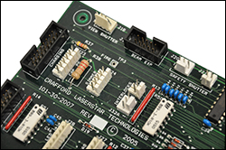 The laser marking of micro components such as silicon wafers and printed circuit boards (PCBs) require traceability throughout the manufacturing process. Marks must be machine-readable, miniaturized and have no negative influence on the manufacturing process. In many cases the laser marking systems have to meet clean room specifications.
When the finished semiconductor components are laser marked, mostly on mold compounds or metal housings, maximum speed is what counts. Precise laser control and high pulse frequencies allow high-contrast laser markings with controlled material penetration depths.
Fiber Laser marking is the most flexible type of direct part marking available in this industry. LaserStar Laser Marking Systems utilize the latest technologies in laser-based material processing. Our Laser markings are permanent, fast, and flexible, allowing for annealing, etching, engraving and surface markings.
Laser marking technology offers significant advantages over traditional marking methods and has the ability to mark a wide variety of materials including metals, anodized metals, coated metals, plastics, ceramics and other materials. Manufacturers currently using laser marking technology are often amazed at how fast and efficient this process is.
Contact LaserStar today to learn more about laser marking semiconductors and other microelectronics.